As I learn more about firmware programming, I happen upon techniques that are not the common for me and my background in sofware applications. Bitwise operators may be used during firmware initialization to configure hardware such as GPIO ports, enable timers and interrupts. Once configured the settings may not be visited again, but when you do, some head scratching may occur repurposing an existing configure:
    /* Step 1: Enable clock for GPIOA and GPIOB */
    RCC_APB2ENR |= (1 << 2);      // Bit 2 (IOPAEN) enables GPIOA peripheral
    RCC_APB2ENR |= (1 << 3);      // Bit 3 (IOPBEN) enables GPIOB peripheral

    GPIOA_CRL &= ~(0xF << 4*0);   // Clear bits 3:0
    GPIOA_CRL |=  (0x2 << 4*0);   // MODE=10 (Output 2 MHz), CNF=00 (Push-pull)
Table of Content
- Function Definition
- Understanding
volatile - Aside: Decoding a Register Definition
- Understanding
const - Understanding the Bitwise Left Shift Operator (
<<) - Understanding the Bitwise OR Operator (
|) - Understanding the Bitwise AND Operator (
&) - Understanding the Bitwise NOT Operator (
~) - Configuring PA0
- Summary
Function Definition
Let’s start with a small program that I wrote for STM32F103xx (Blue Pill) microcontroller, and dive deep into the bitwise operators and bitwise shift operator, plus the ‘volatile’ qualifier.
/* Peripheral Base Addresses */
#define RCC_BASE      0x40021000
#define RCC_APB2ENR   (*(volatile uint32_t *)(RCC_BASE + 0x18))

/* CRL = Configuration Register Low: Controls pins 0–7 */
#define GPIOA_CRL     (*(volatile uint32_t *)(GPIOA_BASE + 0x00))
#define GPIOA_BSRR    (*(volatile uint32_t *)(GPIOA_BASE + 0x10))
#define GPIOA_BRR     (*(volatile uint32_t *)(GPIOA_BASE + 0x14))

#define GPIOB_CRL     (*(volatile uint32_t *)(GPIOB_BASE + 0x00))
#define GPIOB_BSRR    (*(volatile uint32_t *)(GPIOB_BASE + 0x10))
#define GPIOB_BRR     (*(volatile uint32_t *)(GPIOB_BASE + 0x14))

static void GPIO_Init(void);
void delay(volatile uint32_t);

int main(void) {

  GPIO_Init();

    while (1)
    {
        GPIOA_BSRR = (1 << 0);  // Drive PA0 HIGH → LED ON
        GPIOB_BRR  = (1 << 0);  // Drive PB0 LOW  → LED OFF
        delay(500000);

        GPIOB_BSRR = (1 << 0);  // Drive PB0 HIGH → LED ON
        GPIOA_BRR  = (1 << 0);  // Drive PA0 LOW  → LED OFF
        delay(500000);
    }
}

static void GPIO_Init(void) {

    /* Step 1: Enable clock for GPIOA and GPIOB */
    RCC_APB2ENR |= (1 << 2);      // Bit 2 (IOPAEN) enables GPIOA peripheral
    RCC_APB2ENR |= (1 << 3);      // Bit 3 (IOPBEN) enables GPIOB peripheral

    GPIOA_CRL &= ~(0xF << 4*0);   // Clear bits 3:0
    GPIOA_CRL |=  (0x2 << 4*0);   // MODE=10 (Output 2 MHz), CNF=00 (Push-pull)

    GPIOB_CRL &= ~(0xF << 4*0);   // Clear bits 3:0
    GPIOB_CRL |=  (0x2 << 4*0);   // MODE=10 (Output 2 MHz), CNF=00 (Push-pull)
}
Reading from top down, ‘RCC_BASE’ value was determined by reading the STM32F10xxx reference manual. The address ‘0x40021000’ represents the start of RCC register boundary.
/* Peripheral Base Addresses */
#define RCC_BASE      0x40021000
#define RCC_APB2ENR   (*(volatile uint32_t *)(RCC_BASE + 0x18))
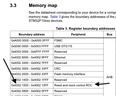
RCC_APB2ENR is 0x18 bits offset from the RCC_BASE.
#define RCC_APB2ENR (*(volatile uint32_t *)(RCC_BASE + 0x18))
Understanding volatile
volatile instructs the compiler not to optimize access to RCC_APB2ENR. Normally, a compiler assumes that a variable only changes when the program modifies it. Hardware registers are different. A peripheral, timer, interrupt controller, or other hardware component may change the value stored at a memory location without the compiler’s knowledge.
In this example, RCC_APB2ENR refers to the Reset and Clock Control (RCC) APB2 Peripheral Clock Enable Register:
#define RCC_APB2ENR (*(volatile uint32_t *)(RCC_BASE + 0x18))
The compiler must perform a real memory access every time the program reads or writes this register. Without volatile, the compiler could cache the register value in a CPU register, remove repeated accesses, or reorder operations. Such optimizations may produce incorrect behavior when communicating with hardware.
The same reasoning applies to the GPIO registers:
#define GPIOA_CRL     (*(volatile uint32_t *)(GPIOA_BASE + 0x00))
#define GPIOA_BSRR    (*(volatile uint32_t *)(GPIOA_BASE + 0x10))
#define GPIOA_BRR     (*(volatile uint32_t *)(GPIOA_BASE + 0x14))
These memory locations correspond to physical hardware. Every write must reach the microcontroller peripheral exactly as written.
Aside: Decoding a Register Definition
Before continuing, let’s quickly unpack this expression:
(*(volatile uint32_t *)(GPIOA_BASE))
Reading from the inside out:
(volatile uint32_t *)(GPIOA_BASE)
casts the address to a pointer to a volatile uint32_t.
*(volatile uint32_t *)(GPIOA_BASE)
then dereferences that pointer, allowing the program to access the 32-bit value stored at that location.
This pattern is commonly used in firmware register definitions:
#define GPIOA_CRL (*(volatile uint32_t *)(GPIOA_BASE + 0x00))
As a result, GPIOA_CRL behaves much like a normal variable:
GPIOA_CRL = 0x02;
However, instead of writing to RAM, the assignment writes directly to a memory-mapped hardware register.
Now, onto ANSI C Type qualifers.
Understanding const
Another ANSI C type qualifier commonly used in firmware is const.
The const qualifier indicates that a value cannot be modified after initialization.
For example:
const uint32_t led_pin = 0;
Attempting to modify led_pin later results in a compiler error:
led_pin = 1; // Error
Firmware projects often use const for:
- Pin assignments
- Register masks
- Lookup tables
- Calibration data
- Configuration values
For example:
const uint32_t GPIOA_CLOCK_ENABLE_BIT = (1 << 2);
Using const communicates intent to both the compiler and future developers. The value is meant to remain unchanged throughout program execution.
It is common to combine const and pointers:
const uint32_t *register_ptr;
This declaration indicates that the data pointed to by register_ptr cannot be modified through the pointer.
Understanding the Bitwise Left Shift Operator (<<)
One of the most frequently used operators in firmware development is the bitwise left shift operator.
The syntax is:
value << shift_count
Each shift moves all bits to the left by the specified number of positions.
For example:
1 << 2
Starting value:
00000001
After shifting left two positions:
00000100
The result is decimal 4.
In firmware, the left shift operator provides a convenient way to create bit masks.
Consider this code:
RCC_APB2ENR |= (1 << 2);
The expression:
(1 << 2)
produces:
00000000000000000000000000000100
Bit 2 is set while all other bits remain cleared.
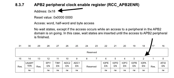
According to the STM32F103 reference manual, bit 2 of the APB2 Peripheral Clock Enable Register is IOPAEN (I/O Port A Clock Enable).
Therefore:
RCC_APB2ENR |= (1 << 2);
enables the clock for GPIOA.
Similarly:
RCC_APB2ENR |= (1 << 3);
creates a mask with bit 3 set, enabling GPIOB through the IOPBEN bit.
Understanding the Bitwise OR Operator (|)
The bitwise OR operator compares two values bit-by-bit.
If either bit is 1, the result is 1.
| Bit A | Bit B | Result |
|---|---|---|
| 0 | 0 | 0 |
| 0 | 1 | 1 |
| 1 | 0 | 1 |
| 1 | 1 | 1 |
Firmware developers commonly use OR operations to set specific bits while leaving all other bits unchanged.
Consider:
RCC_APB2ENR |= (1 << 2);
The |= operator is shorthand for:
RCC_APB2ENR = RCC_APB2ENR | (1 << 2);
Suppose the register currently contains:
00000000
The mask contains:
00000100
The result becomes:
00000100
Only bit 2 changes.
Understanding the Bitwise AND Operator (&)
The bitwise AND operator compares two values bit-by-bit.
A result bit becomes 1 only when both input bits are 1.
| Bit A | Bit B | Result |
|---|---|---|
| 0 | 0 | 0 |
| 0 | 1 | 0 |
| 1 | 0 | 0 |
| 1 | 1 | 1 |
Firmware developers often use AND operations to preserve or isolate specific bits.
Consider:
GPIOA_CRL &= ~(0xF << 4*0);
This line clears the configuration bits associated with PA0 before new settings are applied.
The GPIOA_CRL register is the GPIO Port A Configuration Register Low. It controls pins PA0 through PA7.
Each pin consumes four configuration bits.
For PA0, the configuration occupies bits 3:0.
The expression:
0xF
represents:
1111
Since PA0 starts at bit position 0:
0xF << 0
remains:
0000 1111
Understanding the Bitwise NOT Operator (~)
The bitwise NOT operator inverts every bit.
~0xF
changes:
0000 1111
to:
1111 0000
Applying the NOT operator creates a mask that clears specific bits while preserving all others.
This is exactly what occurs here:
GPIOA_CRL &= ~(0xF << 4*0);
The mask becomes:
1111 1111 1111 1111 1111 1111 1111 0000
When combined with the AND operator, bits 3:0 are cleared.
Configuring PA0
After clearing the existing configuration, the code applies the desired settings:
GPIOA_CRL |= (0x2 << 4*0);
The value:
0x2
is:
0010
According to the STM32F103 reference manual:
MODE = 10
CNF  = 00
This configures PA0 as:
- General-purpose output
- Push-pull output driver
- Maximum speed of 2 MHz
The OR operation inserts these bits into the now-cleared configuration field.
The same process is repeated for PB0 using the GPIOB_CRL register.
Summary
This example introduces several foundational concepts used throughout firmware development:
volatiletells the compiler that hardware may change a value unexpectedly.constprotects values that should never change after initialization.- The left shift operator (
<<) creates bit masks. - The OR operator (
|) sets bits. - The AND operator (
&) preserves or clears selected bits. - The NOT operator (
~) inverts bits and is commonly used when clearing fields.
Once these concepts become familiar, reading microcontroller datasheets and reference manuals becomes much easier. You begin to see registers not as large hexadecimal values, but as collections of individual control bits that can be manipulated with a small set of powerful C operators.