Table of contents
Open Table of contents
Introduction
Before prototyping the controller, it was necessary to re-orient to the way hardware programmed. When the microcontroller first starts up it is necessary to configure the peripherals to support the desired actions.
Initial SOW includes:
- Writing gate status to LCD,
- Driving LED to visual gate status,
- Receving commands to operate gate, and
- Detecting fault status.
Controlling peripherals involues two steps: i.) Configuring registers during startup, and ii.) changing registers values to control external peripherals.
Bare Metal GPIO on STM32
One of the first surprises in bare metal embedded programming is that hardware control does not require special instructions or magical APIs. It looks like C, but it behaves like direct interaction with silicon.
This becomes especially clear when working with GPIO registers such as:
GPIOA_CRL &= ~(0xF << 4*1);
GPIOA_CRL |=  (0x2 << 4*1);
For C programmers, the above code is readable, but will a little foreign for those that write code for desktop applications. Here is a quick orientation to write to hardware.
If you look at typical microcontroller, each pin is labelled with VSS, VDD, PA0, PA1, PB0, etc. These labels originate from manufacturer’s reference manuals. In the case of Blue Pill, STM32F101XX to STM32F103XX, it has several ports with 15 general purpose input / output (GPIO) pins. See section “9.1 GPIO function description” for a succinct explanation.
A key when writing firmware is recognizing GPIO usage structure:
- Memory-mapped registers behave like pointers
- Hardware uses bitfields to pack configuration efficiently
- Clock gating controls whether peripherals are active
- GPIO registers map directly to physical pins
Let’s start with an example code and dissect it:
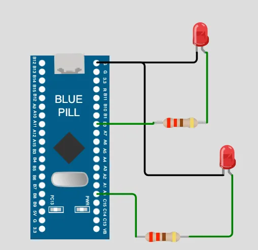
Here is a prototype of a Blue Pill driving two LEDs using GPIO ports A and B, pins 0 for each. The pin labels on the board is PA0 and PB0 respectively:
Here is the bare-metal code to drive the two LEDs.
/* Peripheral Base Addresses */
#define RCC_BASE      0x40021000
#define RCC_APB2ENR   (*(volatile uint32_t *)(RCC_BASE + 0x18))

/* CRL = Configuration Register Low: Controls pins 0–7 */
#define GPIOA_CRL     (*(volatile uint32_t *)(GPIOA_BASE + 0x00))
#define GPIOA_BSRR    (*(volatile uint32_t *)(GPIOA_BASE + 0x10))
#define GPIOA_BRR     (*(volatile uint32_t *)(GPIOA_BASE + 0x14))

#define GPIOB_CRL     (*(volatile uint32_t *)(GPIOB_BASE + 0x00))
#define GPIOB_BSRR    (*(volatile uint32_t *)(GPIOB_BASE + 0x10))
#define GPIOB_BRR     (*(volatile uint32_t *)(GPIOB_BASE + 0x14))

static void GPIO_Init(void);
void delay(volatile uint32_t);

int main(void) {

  GPIO_Init();

    while (1)
    {
        GPIOA_BSRR = (1 << 0);  // Drive PA0 HIGH → LED ON
        GPIOB_BRR  = (1 << 0);  // Drive PB0 LOW  → LED OFF
        delay(500000);

        GPIOB_BSRR = (1 << 0);  // Drive PB0 HIGH → LED ON
        GPIOA_BRR  = (1 << 0);  // Drive PA0 LOW  → LED OFF
        delay(500000);
    }
}

static void GPIO_Init(void) {

    /* Step 1: Enable clock for GPIOA and GPIOB */
    RCC_APB2ENR |= (1 << 2);      // Bit 2 (IOPAEN) enables GPIOA peripheral
    RCC_APB2ENR |= (1 << 3);      // Bit 3 (IOPBEN) enables GPIOB peripheral

    /* Step 2: Configure PA0 and PB0 as Output Push-Pull
      Each pin uses 4 bits. Pin 0 → shift by (0 × 4) = 0 bits
       MODE = 10 → Output 2 MHz
       CNF  = 00 → Push-pull
    */

    GPIOA_CRL &= ~(0xF << 4*0);   // Clear bits 3:0
    GPIOA_CRL |=  (0x2 << 4*0);   // Set MODE=10, CNF=00

    GPIOB_CRL &= ~(0xF << 4*0);   // Clear bits 3:0
    GPIOB_CRL |=  (0x2 << 4*0);   // Set MODE=10, CNF=00
}

void delay(volatile uint32_t count) {
    while (count--);
}
To use a GPIO port pin, the entire port must be enabled using the Reset and clock control register (RCC). The reference manual specifies the RCC start address is: 0x40021000.
#define RCC_BASE 0x40021000
Next step is to enable one of the internal clocks for the desired GPIO port(s), we enabled the port via one of the internal clocks, in this case the fast peripheral APB2:
                RCC (clock controller)
                      |
      -----------------------------------
      |               |                 |
    AHB             APB1              APB2
 (fast core)   (slow peripherals)  (fast peripherals)
The following code enables GPIO ports A and B on the fast peripherals clock:
 /* Step 1: Enable clock for GPIOA and GPIOB */
 RCC_APB2ENR |= (1 << 2);      // Bit 2 (IOPAEN) enables GPIOA peripheral
 RCC_APB2ENR |= (1 << 3);      // Bit 3 (IOPBEN) enables GPIOB peripheral
This is achieved by offsetting 0x18 bits from RCC_BASE base address:
#define RCC_APB2ENR (*(volatile uint32_t *)(RCC_BASE + 0x18))
An aside: why volatile? Without volatile, the compiler might assume repeated reads return the same value and silently remove operations. That would break hardware interaction entirely.
Now that GPIO ports A and B are enabled with the fast peripheral clock, the next step is to configure the individual pin. As per the reference manual, the configuration register low
 GPIOA_CRL &= ~(0xF << 4*0);   // Clear bits 3:0
 GPIOA_CRL |=  (0x2 << 4*0);   // MODE=10 (Output 2 MHz), CNF=00 (Push-pull)
The first line clears the bits 3:0
xxxx xxxx xxxx xxxx xxxx xxxx xxxx 0000
and the second line configures MODE and CNF:
xxxx xxxx xxxx xxxx xxxx xxxx xxxx 0010
MODE controls whether a pin is an input or output and its output speed. CNF (Configuration) specifies the electrical behavior of the pin, such as push-pull, open-drain, or alternate function. The final configuration becomes MODE=10 and CNF=00. NOTE: The second line only writes the MODE bits because the CNF bits were already cleared by the first line.
The GPIOA_CRL is defined 0x00 bits offset from the GPIOA_BASE
 #define GPIOA_CRL     (*(volatile uint32_t *)(GPIOA_BASE + 0x00))
 #define GPIOA_BSRR    (*(volatile uint32_t *)(GPIOA_BASE + 0x10))
 #define GPIOA_BRR     (*(volatile uint32_t *)(GPIOA_BASE + 0x14))
The same pattern is repeated for GPIOB_CRL.
With ports configured by the GPIO_Init() function, the while loop alternately drives the pins high and low to turn on or off the LED:
int main(void) {

  GPIO_Init();

    while (1)
    {
        GPIOA_BSRR = (1 << 0);  // Drive PA0 HIGH → LED ON
        GPIOB_BRR  = (1 << 0);  // Drive PB0 LOW  → LED OFF
        delay(500000);

        GPIOB_BSRR = (1 << 0);  // Drive PB0 HIGH → LED ON
        GPIOA_BRR  = (1 << 0);  // Drive PA0 LOW  → LED OFF
        delay(500000);
    }
}
The driving of two LEDs is basic, however, understanding how to enable ports and configure pins now empowers us to further configure ports and pins to control our project.