Table of contents
Open Table of contents
Introduction
This post continues from Part 3 by configuring the Blue Pill (STM32F103xx) to drive an external peripheral, specifically a 1602A-A LCD. The purpose of this article is to code and wire such that text can be written to and displayed on the LCD. In future articles, the code will be updated to display status codes for debugging and operational information.
To follow along, have the STM32F103xx Reference Manual available and a reference manual for a 16 x 2 LCD. My LCD has an HD44780U chip. This reference manual will do for our purpose: HD44780U (LCD-II)
Like the LED setup, I’ll post the completed working code here, and if you want to learn more, see explanations below:
/* =========================================================
   STM32F103 (Blue Pill)
   Goal: Display text in LCD
   Documentation:
   - https://stm32-base.org/boards/STM32F103C8T6-Blue-Pill.html
   - RM0008 Reference manual
   - LCD manual - https://cdn.sparkfun.com/assets/9/5/f/7/b/HD44780.pdf
   ========================================================= */

/* Peripheral Base Addresses */
#define RCC_BASE      0x40021000
#define RCC_APB2ENR   (*(volatile uint32_t *)(RCC_BASE + 0x18))

/* GPIOA_CRL - Configuration Register Low: pins PA0–PA7 */
/* Use pins PA0 - PA7 to connect with LCD pins D0-D7.   */
/* D0 is LSB and D7 MSB */
#define GPIOA_BASE    0x40010800
#define GPIOA_CRL     (*(volatile uint32_t *)(GPIOA_BASE + 0x00))
#define GPIOA_ODR     (*(volatile uint32_t *)(GPIOA_BASE + 0x0C))
#define GPIOA_BSRR    (*(volatile uint32_t *)(GPIOA_BASE + 0x10))
#define GPIOA_BRR     (*(volatile uint32_t *)(GPIOA_BASE + 0x14))

/* GPIOB_CRL - Configuration Register Low: pins PB0–PB7 */
#define GPIOB_BASE    0x40010C00
#define GPIOB_CRL     (*(volatile uint32_t *)(GPIOB_BASE + 0x00))
#define GPIOB_BSRR    (*(volatile uint32_t *)(GPIOB_BASE + 0x10))
#define GPIOB_BRR     (*(volatile uint32_t *)(GPIOB_BASE + 0x14))

/* PB0 -> RS, PB1 -> RW, PB2 -> EN */
/* We control when LCD reads input using Enable changing edge. */

#define RS (1 << 0)
#define EN (1 << 1)
#define RW (1 << 2)       // For now, direct to GND

static void LCD_Init(void);
static void LCD_Instruction(uint8_t cmd);
static void LCD_Data(char *data);
static void LCD_Enable();

void theDelay(volatile uint32_t);

int main(void) {

  LCD_Init();

  while (1)
  {
    LCD_Data("  Hello World!");
    theDelay(500000);
    LCD_Instruction(0x01); // clear display
  }
}

static void LCD_Init(void) {

  /* Step 1: Enable clock for GPIOA */
  /* GPIO port bus, used for data   */
  RCC_APB2ENR |= (1 << 2);      // Bit 2 (IOPAEN) enables GPIOA port

  // Set pins PA0 - PA7 as output, push-pull
  for (int pin = 0; pin < 8; pin++) {
    GPIOA_CRL &= ~(0xF << (4 * pin)); // Clear 4 bit range
    GPIOA_CRL |=  (0x2 << (4 * pin)); // MODE=10 (Output 2 MHz), CNF=00 (Push-pull)
  }
  /* Step 1: Enable clock for GPIOB */
  /* Used to control RS, RW, EN     */
  RCC_APB2ENR |= (1 << 3);      // Bit 3 (IOPBEN) enables GPIOB peripheral

    for (int pin = 0; pin < 3; pin++) {
    GPIOB_CRL &= ~(0xF << (4 * pin)); // Clear 4 bit range
    GPIOB_CRL |=  (0x2 << (4 * pin)); // MODE=10 (Output 2 MHz), CNF=00 (Push-pull)
  }

  theDelay(50000);

  LCD_Instruction(0x38); // function set
  LCD_Instruction(0x08); // display off
  LCD_Instruction(0x01); // clear display
  theDelay(2000);
  LCD_Instruction(0x06); // entry mode
  LCD_Instruction(0x0C); // display on
}

static void LCD_Instruction(uint8_t cmd) {

    GPIOB_BRR = RS;      // Command mode
    GPIOB_BRR = RW;      // Write mode

    GPIOA_ODR = cmd;     // Put byte on data bus

    LCD_Enable();
}

static void LCD_Data(char *data)
{
    while (*data)
    {
        GPIOB_BSRR = RS;     // RS = 1 (data mode)
        GPIOB_BRR  = RW;     // RW = 0 (write mode, optional if RW tied low)

        GPIOA_ODR = (uint8_t)(*data);  // put ASCII byte on bus

        LCD_Enable();       // latch into LCD

        data++;             // next character
    }
}

static void LCD_Enable(void)
{
    GPIOB_BRR = EN;   // Ensure E starts low
    GPIOB_BSRR = EN;  // E high
    theDelay(100);

    GPIOB_BRR = EN;   // E low
    theDelay(100);
}

void theDelay(volatile uint32_t count) {
  while (count--);
}
There is too much code for one file. In future updates I’ll create lcd.c and lcd.h files for the LCD code, but for now, I’ll keep in one file (works more easly with the simulator being used).
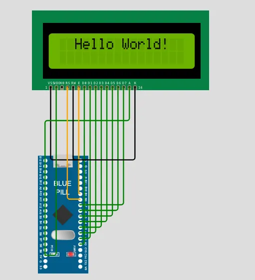
Hardware Mapping
The LCD is configured in 8-bit mode. The 1602A LCD supports 4-bit mode too, but for my initial implementation, 8-bit mode is used. The LCD pins can be grouped as: Data bus and Control signal type pins.
Data bus (Port A)
Microcontroller Port A will be used for the 8-bit mode wiring. This maps microcontroller pins PA0–PA7 to LCD pins D0–D7
Port A has 16 pins: 8 low-register pins and 8 high-register pins.
Control signals (Port B)
The PB0-PB2 pins are used to set the LCD mode, either instruction mode or data mode.
- PB0 → RS (Register Select)
- PB1 → EN (Enable)
- PB2 → RW (Write control, currently unused and tied low in practice)
If your LCD manual includes a timing characteristics diagram, locate the E line and see how a rising edge, and possibly a falling edge, causes the LCD to access the DB0 - DB7 pins. E signal triggers when data is read.
This separation is intentional:
- Port A acts as a pure 8-bit data bus
- Port B handles control flow and signal interpretation
Core Concept: Writing a Byte to the LCD
The LCD uses a simple parallel interface:
- Place an 8-bit value on the data bus (PA0–PA7)
- Configure control signals (RS, RW)
- Pulse EN to trigger LCD read
The EN signal acts as a latch clock for the LCD.
Atomic vs Full-Port Operations
A key design decision in this implementation is the distinction between atomic bit operations and full-port writes.
Atomic control signals (BSRR / BRR)
Control pins use atomic operations:
GPIOB_BSRR = RS;   // set RS high
GPIOB_BRR  = RW;   // set RW low
These operations:
- affect only selected bits
- do not depend on current register state
- avoid read-modify-write hazards
This makes them ideal for control signals such as RS, RW, and EN.
Full-port data writes (ODR)
The data bus uses a full register write:
GPIOA_ODR = (uint8_t)(*data);
This writes all 8 bits at once to PA0–PA7. Each pin directly represents one bit of the ASCII character. For example, ASCII ‘A’ = 0x41 = 0100 0001
PA7 PA6 PA5 PA4 PA3 PA2 PA1 PA0
0   1   0   0   0   0   0   1
This ensures the LCD always sees a valid, stable byte when EN is triggered.
LCD Enable Pulse
The LCD only reads data when EN transitions.
static void LCD_Enable(void)
{
    GPIOB_BRR = EN;   // ensure low
    GPIOB_BSRR = EN;  // rising edge
    theDelay(100);

    GPIOB_BRR = EN;   // falling edge (latch)
    theDelay(100);
}
This pulse acts as the clock signal for the LCD interface.
Instruction Write
Instructions configure LCD behaviour:
static void LCD_Instruction(uint8_t cmd)
{
    GPIOB_BRR = RS;   // command mode
    GPIOB_BRR = RW;   // write mode

    GPIOA_ODR = cmd;  // send instruction byte

    LCD_Enable();
}
Common instructions include:
- 0x01 → Clear display
- 0x06 → Entry mode set
- 0x0C → Display ON
- 0x38 → Function set (8-bit, 2-line)
Data Write
Character output is handled byte-by-byte:
static void LCD_Data(char *data)
{
    while (*data)
    {
        GPIOB_BSRR = RS;               // data mode
        GPIOB_BRR  = RW;               // write mode

        GPIOA_ODR = (uint8_t)(*data);  // ASCII byte on bus

        LCD_Enable();

        data++;
    }
}
Each character is latched into LCD memory on the EN pulse.
Initialization Sequence
The LCD must be initialized after power-up in a specific order:
theDelay(50000);

LCD_Instruction(0x38); // function set
LCD_Instruction(0x08); // display off
LCD_Instruction(0x01); // clear display

theDelay(2000);
LCD_Instruction(0x06); // entry mode set
LCD_Instruction(0x0C); // display on
Without this sequence, the LCD may display undefined characters or remain blank.
Main Loop Behaviour
For now, the system continuously writes and clears a message:
while (1)
{
    LCD_Data("  Hello World!");
    theDelay(500000);
    LCD_Instruction(0x01); // clear display
}
This is a functional test to confirm:
- correct GPIO configuration
- correct timing
- correct LCD initialization
- correct enable pulse behaviour
Design Improvements Introduced
- Symbolic pin definitions
#define RS (1 << 0)
#define EN (1 << 1)
#define RW (1 << 2)
This removes magic numbers and makes signal intent explicit.
- Separation of data and control planes
- Port A → 8-bit data bus
- Port B → control signals
- This mirrors real hardware bus design and improves clarity.
- Mixed register strategy
- BSRR / BRR → atomic control operations
- ODR → full parallel data bus write
Each register type is used according to its role.
Key Concept Summary
The LCD driver works because each layer matches hardware behaviour:
- GPIOA_ODR represents a full 8-bit electrical bus
- GPIOB_BSRR/BRR provides atomic control signalling
- EN pulse acts as the synchronisation clock
- RS determines interpretation of the byte